Recent research on optical phenomena in multilayer metamaterials
Recent years have seen incredible advances in fundamental research related to photonics. This has been made possible both by new research tools allowing the fabrication and characterization of photonic structures and because of the development of advanced methods of computational electrodynamics, which have proved crucial to understanding physical phenomena at the micro and nanoscale. On these foundations, the concept of metamaterials was born. These are structures whose unique optical properties are more related to the geometrical arrangement of the sub-wavelength size of the elements than to the properties of the constituent materials used.
The subject of metamaterials has become one of the most exciting issues in modern optics. The ability to receive, modulate or emit electromagnetic waves is the operating principle of countless technological devices that underpin the modern world. These include ultrafast light modulators, tunable frequency filters, or devices using electrically controlled non-linear effects.
Our studies of optical phenomena in multilayer metamaterials thematically cover a variety of scientific topics, ranging from linear and non-linear optics to the concept of metamaterials and semiconductor physics. They give us insights into the interactions of light with accumulation layers in multilayer geometries. They deepen our understanding of the formation of accumulation layers of carriers and interfacial processes. We study the issue of electrically tuned metamaterials both theoretically, numerically, and experimentally in our Photonic and Plasmonic Nanostructures Laboratory.
The starting point of our research is the phenomenon of the formation of a carrier accumulation layer at the interface between the dielectric oxide and the semiconductor. Such a layer is formed if the material containing the semiconductor-dielectric interface is placed in an external electric field. Our main objective is to investigate how the electrically controlled accumulation layer formation process affects the linear and non-linear optical properties of a metallic-dielectric-semiconductor multilayer metamaterial. We aim to demonstrate that the unique characteristics of metamaterials, such as e.g. spatial and temporal frequency filtering, hyperbolic dispersion, super-resolution imaging, total absorption, or non-linear properties, can be modified over the entire spectral range (i.e. from visible light to infrared) with only an applied voltage.
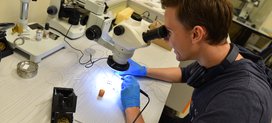
Alexander Korneluk, one of our PhD students from the Information Optics Department, under the supervision of dr Tomasz Stefaniuk, has already fabricated the first working multilayer structures. Tests using an ellipsometer, i.e. a device that determines the optical properties of a material on the basis of the polarisation state of light, have shown that in the formed accumulation layer, changes in the refractive index value of 0.35 at a wavelength of 1500 nm and a 50% change in carrier concentration at 2.5V have been achieved. In comparison, the changes that are obtained in the usual materials used in optical modulators are 100 to 100,000 times weaker.
Originally published on - Oct. 26, 2022, noon
Last update on - March 20, 2023, 2:52 p.m.
Publisher - Sekretariat IGF

